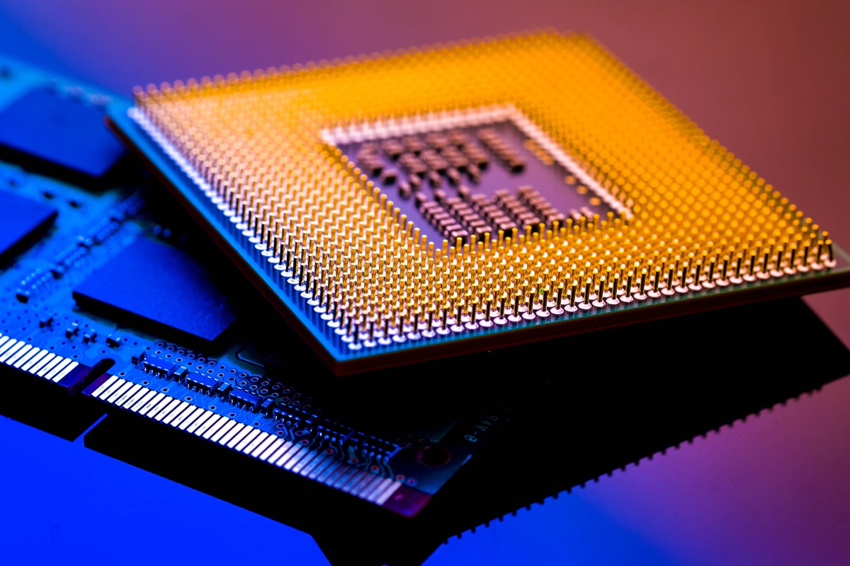
Ion implantation is a key process in the fabrication of semiconductor devices, playing a crucial role in tailoring the electrical properties of materials used in chip production. As the semiconductor industry continues to advance, driven by the demand for smaller and more efficient devices, the importance of precise ion implantation has only grown. Ion implantation allows manufacturers to embed ions into a semiconductor substrate, altering its characteristics to meet specific needs, such as optimizing transistor performance or reducing power consumption. Erik Hosler, an expert in semiconductor metrology, mentions that this technique is indispensable in the production of advanced chips.
How Ion Implantation Shapes Semiconductor Materials
Ion implantation is critical in shaping semiconductor materials at the nanoscale, allowing for incredible precision in the modification of electrical properties. It ensures that ions are deposited at specific depths and concentrations, which is essential as the industry pushes toward smaller transistor sizes, with chips shrinking to as small as 3 nanometers. The process is integral to modern chip production because it enables manufacturers to manipulate the behavior of semiconductor materials, thereby enhancing the overall performance and efficiency of the final product.
Precision and Performance in Modern Chip Production
One of the most significant advantages of ion implantation is its precision. The ability to control ion placement with such accuracy allows manufacturers to optimize the electrical properties of semiconductor devices, ensuring consistent performance across increasingly smaller chip designs.
This precision is especially vital as industries continue to push the boundaries of technology, demanding faster and more efficient chips. By leveraging ion implantation, manufacturers can fine-tune transistor behavior, enhancing both speed and power efficiency.
Erik Hosler notes, “Accelerator technologies, particularly in ion implantation, are enabling manufacturers to push the limits of miniaturization while maintaining the integrity of semiconductor devices.”
Innovation and the Future of Semiconductor Devices
Furthermore, ion implantation not only enhances the performance of individual semiconductor devices but also accelerates the innovation cycle in chip production. With the ability to quickly modify and test new materials, manufacturers can rapidly adopt cutting-edge technologies, reducing production costs and improving yields. This capacity for innovation is essential in a competitive industry where faster, more efficient chips are in constant demand.
Ion implantation is an indispensable technology in semiconductor device fabrication. It allows for the precise modification of semiconductor materials, which plays a crucial role in the development of faster, smaller, and more efficient chips. As accelerator technologies continue to evolve, ion implantation will remain a cornerstone of semiconductor innovation, shaping the future of electronics in a world increasingly reliant on high-performance computing and advanced technologies.